Shenzhen ATFU Electronics Technology ltd

Shenzhen ATFU Electronics Technology LTD

Manufacturer from China
Active Member
6 Years
Home / Products / Amplifier IC Chip /

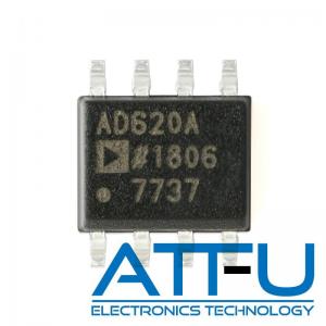
Low Power Amplifier IC Chip Small Footprint Design AD620ARZ-REEL7 With External Resistor

Contact Now
Shenzhen ATFU Electronics Technology ltd
City:shenzhen
Province/State:guangdong
Country/Region:china
Contact Person:MissMia
Contact Now

Low Power Amplifier IC Chip Small Footprint Design AD620ARZ-REEL7 With External Resistor

Ask Latest Price
Video Channel
Brand Name :ADI
Model Number :AD620ARZ-REEL7
Certification :ROHS
Place of Origin :Original Factory
MOQ :10pcs
Price :Negotiate
Payment Terms :T/T, Western Union,Paypal
Supply Ability :100000pcs
Delivery Time :1-3Days
Packaging Details :BOX
Series :AD620ARZ
Package :SOP8
Feature :Instrumentation Amplifier
Application :MOS clock timers
Voltage Range :4.6V ~ 36V, ±2.3V ~ 18V
Current :Low Power Consumption
more
Contact Now

Add to Cart

Find Similar Videos
View Product Description

AD620ARZ-REEL7 Amplifier IC Chip Low Power Instrumentation 1 Circuit 8-SOIC

low drift, low power, high accuracy, and is ideal for high-precision applications

Description:

AD620 comes in 8-lead SOIC and DIP packages and are low-cost, high-accuracy instrumentation amplifiers that, with an external resistor, allow the user to set gains of 1 to 10,000. The small footprint design and low power consumption (only 1.3 mA (maximum) supply current) make it a good fit for portable or remote applications that require a battery.

The AD620, with its high accuracy of 40 ppm (maximum) nonlinearity, low offset voltage of 50 µV (maximum), and offset drift of 0.6 µV/°C (maximum), is ideal for use in precision data acquisition systems such as weigh scales and transducer interfaces. Furthermore, the low noise, low input bias current, and low power of the AD620 make it well suited for medical applications such as ECG and noninvasive blood pressure monitors.

The low input bias current of 1.0 nA (maximum) is made possible with the use of Superϐeta processing in the input stage. The AD620 works well as a preamplifier due to its low input voltage noise of 9 nV/√Hz at 1 kHz, 0.28 μV p-p in the 0.1 Hz to 10 Hz band, and 0.1 pA/√Hz input current noise. Also, the AD620 is well suited for multiplexed applications with its settling time of 15 μs to 0.01%, and its cost is low enough to enable designs with one in-amp per channel.

Features
  • Easy to use
  • Gain range of 1 to 10,000 with one external resistor
  • Wide power supply range (±2.3 V to ±18 V)
  • Higher performance than three op amp IA designs
  • Low power, 1.3 mA (max.) supply current
  • 50 μV (max.), input offset voltage
  • 0.6 μV/°C (maximum) input offset drift
  • 1.0 nA (max.), input bias current
  • 100 dB (min.) common-mode rejection ratio (G = 10)
  • Low noise
  • 9 nV/√Hz at 1 kHz input voltage noise
  • 0.28 μV p-p noise (0.1 Hz to 10 Hz)
  • 120 kHz bandwidth (G = 100)
  • 15 μs settling time to 0.01%


Applications

Application areas include limit comparators, simple analog to digital converters; pulse, squarewave and time delay generators; wide range VCO; MOS clock timers; multivibrators and high voltage digital logic gates.


• Battery Powered Applications
• Industrial Applications

Inquiry Cart 0